Devices
This area covers the aspects of analysis, design, prototyping and experimental characterization of a wide range of electronic and photonic devices that find applications in various systems in the field of electronics, communication engineering, bio-engineering and industrial manufacturing.
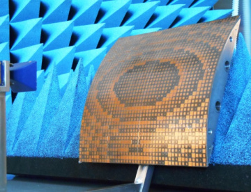
The DET has a consolidated tradition in the design and analysis of innovative Antennas and Microwave Devices. The activity on antennas involves several aspects, including the design of small antennas, wearable/textile antennas, reflectarrays and transmitarray, multi-frequency and reconfigurable antennas. They cover different fields of applications, as satellite communication systems, radar and imaging sytems, and the ranges of frequencies from microwaves up to millimeter waves and subTHz. From a technological point of view, solid competences relating to the design and manufacturing of both antennas and microwave devices, have been developed: they cover more assessed techniques as the realization of waveguide or microstrip techniques, but also more innovative one, as the 3D manufacturing of both plastic and metallic components and the nanotechnology. In parallel, DET researchers are also expert on the development of efficient numerical tools for the pre-prototyping, the optimization and the analysis of antennas. In the frame of microwave devices, the groups involved have a long tradition in developing numerical techniques for the efficient simulation of devices: in the years, they implemented tools for analyzing the device variability through physics-based models, methods for the generation of compact models of complex linear and non-linear dynamic circuits, as well as for the characterization of the effects of natural randomicity of parameters and of noise in microwave devices and circuits. Characterization of microwave devices and circuit is also available.
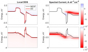
The research on Photonic Devices is oriented to the development of simulation tools and design methods of various optoelectronic components such as semiconductor edge emitting lasers and VCSELS at optical communication wavelengths, Quantum Cascade lasers, visible and UV LEDs, photodetectors for far infra-red image sensors, solar cells and various types of optical modulators . The modelling of some of these devices is also based on a multi-physics approaches combining self-consistently rigorous microscopic description of modern materials, solution of the carrier transport equations, full-wave electromagnetic solvers and thermal models.
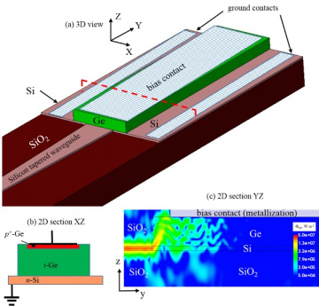
An important field is also the research on active and passive photonic devices for integration in Silicon Photonic platform with main application to optical interconnects. This activity covers all the transceiver and receiver components including design of hybrid Si/III-V lasers, Si-Ge photodetectors as well as design and mask layout of passive components. Experimental characterization of the devices is available in the Interdipertimental Center PhotoNext which is equipped with the instruments required for testing, even when the devices are in a prototypal version and thus require sub-micrometer accuracy in free space alignment.
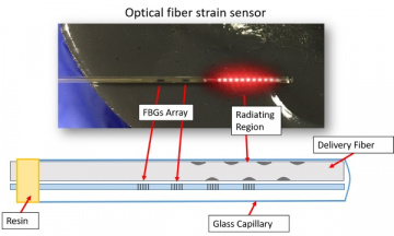
In the field of Sensors, the Department develops in collaboration with DISAT thin film sensors realized with Plasma Enhanced Chemical Vapor Deposition, optical sensors for the realization of networks of distributed sensor and CMOS current sensors integrated in high power transistors; moreover, it is active on the design of innovative sensors for biomedical applications, for tagless people localization, for monitoring envirnmental conditions and for other applications.
In collaboration with DISAT, IIT and INRIM, DET covers a few aspect of Nanotechnologies that include the RF characterization of graphene and carbon nano-tubes, nano-magnetic logics and silicon nanowires. Tools for the analysis of nano-devices, eventually based on organic and bio-molecules, have been developed, using physical level and/or high level simulation models.